- Python 86.2%
- Nix 12.6%
- Ruby 0.9%
- HTML 0.3%
| .claude/skills/kicad-schematic-from-reference | ||
| docs | ||
| img | ||
| kicad | ||
| migration | ||
| pkgs | ||
| script | ||
| svg | ||
| .gitignore | ||
| COPYING | ||
| default.nix | ||
| flake.lock | ||
| flake.nix | ||
| README.md | ||

NixOS Badge
This repo contains KiCad files and Nix expressions for fabricating the NixOS Badge using PCBWay.
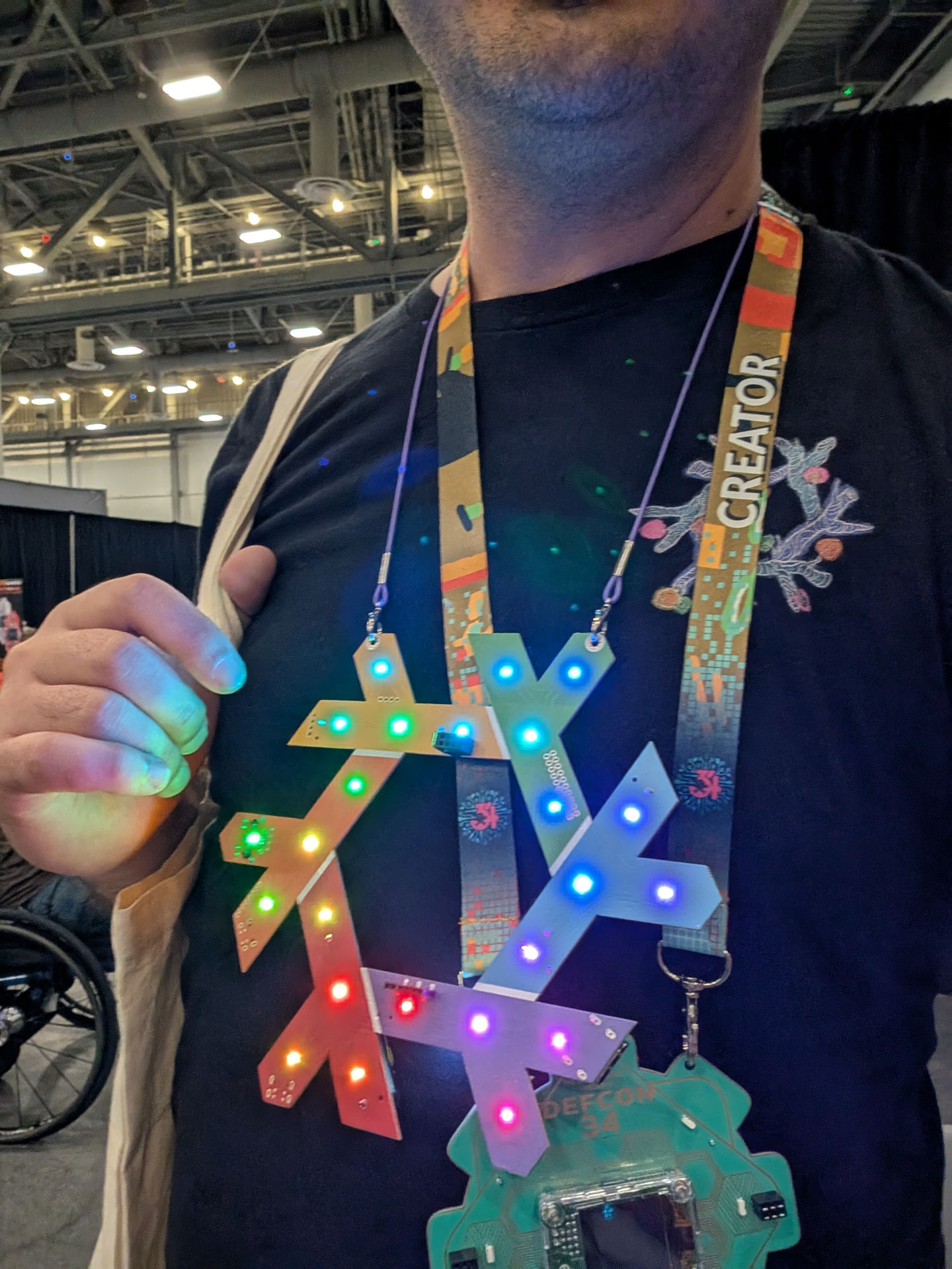
Developing
nix develop
Note that you will need a machine with a reasonably good GPU to edit the board. The artwork makes a recent AMD or NVIDIA chip a necessity.
Don't try to understand the routing, you will go mad
Building
nix build ^*ornix build .#render^*- Gerbers are in
result - Fab output (
nixos_1.zipGerber archive;bom.csvandpositions.csvfor placement) are inresult-fab- This is repackaged to
nixos_1.7zto fit PCBWay's file upload service
- This is repackaged to
- Renders are in
result-renderif you want a render - DRC and ERC checks are in
result-check
- Gerbers are in
Nix Flake Logo
Use NixOS/branding and produce the output
.#nixos-branding.artifacts.internal.nixos-logomark-default-gradient-none.
Reference design
- The closest reference design is included in the accompanying materials for the duo-module-01.
- The DSI/HDMI bridge was based on a design by Olimex, released under CERN Open Hardware License v2 (Strongly Reciprocal)
Fabrication playbook
Unfortunately you can't just deploy-rs to PCBWay but we can get close.
- Upload the gerber bundle
- Configure fabrication options
- Base material: FR4
- Delivery Format: Single PCB (panels were actually more expensive)
- Color: White
- Thickness: 1.6mm
- Tracks: 4/4mil
- Surface finish: ENIG
- Silkscreen: Colorful, dual-sided
- Vias: Untented
- Min via hole size: 0.3mm
- Include product number: Specify location ("WayWayWay" silkscreen on back)
- Configure assembly options
- Assembly Side: both sides
- Upload bom.csv and positions.csv from the fab output as BOM and centroid files
- Note that a couple components are deliberately left out
Lead time is expected to be at least ~20 days (double badge v1 in this economy).
Things we know work
- Battery power (you can get a few hours out of it, but it can be very battery hungry)
- Bling (note that if the battery gets low it becomes red glitch art -- the LEDs are connected to VSEL instead of the 3.3v buck, this was mostly a deliberate design choice because the cosmetic effects are interesting)
- Serial through the CH347 (works great)
- Both ARM and RISC-V boot
- SD card works (some higher speed ones may have trouble, YMMV)
- Ethernet and USB work fine
Things that have not been tested
- HDMI (needs a kernel driver port for the DSI out)
- USB-C mode switching
- JTAG (CH347 serial supports it, we could use an OpenOCD config)
- ARM/RISC-V persistent latch for AUTO mode
Things that need software support
(see https://github.com/NixVegas/BadgeOS)
- WiFi (kernel driver needs rebase from 5.10 though we have the bootrom)
- TPU (0.5 TOPS, tested with debian but drivers need forward port)
- RISC-V little core
- SAO (likely enable in device tree)
- Voltage measurement ADCs
We recommend pointing your LLM of choice at this repo and your hardware to work through the gnarly driver porting. We're doing it.
Trimmings
Please use this badge in ways we could never have imagined, but these are the intended ways:
- CPU. We got the Duo Modules from the eval boards, hotplated them off at 360C, and precision hand soldered them.
- We ended up with 80% yield Friday of DEF CON
- Battery holders (BA1AAPC)
- Batteries (ton of AA from Amazon)
- Lanyards (search Amazon for facemask lanyards, they need to have the right clasp)
- Ethernet magjacks, supercaps for RTC circuit, SAO connectors, and LCDs: find them on Amazon and AliExpress
- Supercap is an Amefil H-5.5V0.33F-10P horizontal button cell supercap
- The SAO connector is a 6 pin female header (keyed), see here
- The OLED connector is made for a 4-pin I2C OLED. We suggest a 4 pin header if you'd like to interface with it, otherwise you will permanently cover up a LED by soldering it to the front. Both vertical and horizontal pinouts are supported:
- The front pin header is meant for a Sharp Memory Display.
- You may have to remove the tantalum decoupling caps at the ethernet center taps. They break the ethernet connection. All released badges have this done already (known issue with the component placement).